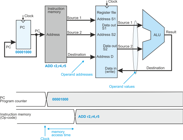
The timing diagram shows the output of the instruction memory. This contains the operation ADD r2,r4,r5 which is maintained for the remainder of this clock cycle.
Executing an instruction step-
The contents of the program counter, in this case 00001000, interrogate the instruction memory to read the instruction at that address. In this case the instruction is ADD r2,r4,r5.
The output of the instruction memory will consist of the bits of the instruction
that define the operation, the op-
The other bits of the instruction are the two source operand addresses corresponding to registers r4 and r5, and the destination operand corresponding to register r2.